
nowornever
Shift Register (쉬프트 레지스터) 역할 본문
쉬프트 레지스터에 대해 알아봅시다. (번역 자료입니다)
쉬프트 레지스터(Shift Register) 는 카운터와 같이 순차적 논리(sequential logic) 의 한 종류입니다. combinational logic 과 달리 sequential logic 은 현재의 입력뿐 아니라 과거의 입력에도 영향을 받습니다. 다시 말하면 sequential logic 은 과거의 event 를 기억하게 되는거죠.
Shift register 는 이산적인(discrete) 디지털 신호나 waveform(파형)을 공급합니다. 파형은 클럭에 동기화되어 반복적인 square wave(구형파) 가 "n" 번의 이산적인 클럭 횟수만큼 delay(지연) 되는 것입니다. 여기서 "n"은 shift register 의 stage 들의 개수를 의미합니다. 따라서, 4개의 stage 를 가진 shift register 는 "data in" 을 "data out" 으로부터 4 클럭 만큼 지연시킵니다. Shift register 에 있는 stage 들은 지연 stage (delay stages) 입니다. 일반적으로 "D" 타입의 Flip-Flop 혹은 "JK" 타입의 Flip-Flop 들로 구성되어 있지요.
이전에는 아주 긴 (몇백 스테이지의) 쉬프트 레지스터들은 디지털 메모리의 역할을 했다고 합니다. 이런 구식의 어플리케이션은 초기 컴퓨터 메모리로 사용되었던 acoustic mercury delay line 을 연상케 합니다. (응???)
시리얼 데이터 전송에서 쉬프트 레지스터는 몇미터부터 몇 킬로미터의 거리까지 parallel data 를 serial form 으로 바꾸기 위해 사용됩니다. 특히 serial 데이터 통신은 느린 parallel data 전선들을 하나의 선으로 아주 빠른 스피드의 회로로 바꾸어 줍니다. 대단하죠 ?
또, 몇십센티미터길이의 짧은 거리에서의 serial data 통신은 마이크로프로세서에서 데이터를 받아내거나 공급하기 위해 쉬프트 레지스터를 사용합니다. ADC(아날로그 디지털 변환기), DAC(디지털 아날로그 변환기), display driver, 그리고 메모리 등 수많은 주변기기(peripheral)들 또한 circuit board(회로보드) 안에서 쓰는 양 (amount of writing) 을 줄이기 위해 쉬프트 레지스터를 사용합니다.
Some specialized counter circuits actually use shift registers to generate repeating waveforms. Longer shift registers, with the help of feedback generate patterns so long that they look like random noise, pseudo-noise.
Basic shift registers are classified by structure according to the following types:
- Serial-in/serial-out
- Parallel-in/serial-out
- Serial-in/parallel-out
- Universal parallel-in/parallel-out
- Ring counter

Above we show a block diagram of a serial-in/serial-out shift register, which is 4-stages long. Data at the input will be delayed by four clock periods from the input to the output of the shift register.
Data at "data in", above, will be present at the Stage A output after the first clock pulse. After the second pulse stage A data is transfered to stage B output, and "data in" is transfered to stage A output. After the third clock, stage C is replaced by stage B; stage B is replaced by stage A; and stage A is replaced by "data in". After the fourth clock, the data originally present at "data in" is at stage D, "output". The "first in" data is "first out" as it is shifted from "data in" to "data out".

Data is loaded into all stages at once of a parallel-in/serial-out shift register. The data is then shifted out via "data out" by clock pulses. Since a 4- stage shift register is shown above, four clock pulses are required to shift out all of the data. In the diagram above, stage D data will be present at the "data out" up until the first clock pulse; stage C data will be present at "data out" between the first clock and the second clock pulse; stage B data will be present between the second clock and the third clock; and stage A data will be present between the third and the fourth clock. After the fourth clock pulse and thereafter, successive bits of "data in" should appear at "data out" of the shift register after a delay of four clock pulses.
If four switches were connected to DA through DD, the status could be read into a microprocessor using only one data pin and a clock pin. Since adding more switches would require no additional pins, this approach looks attractive for many inputs.
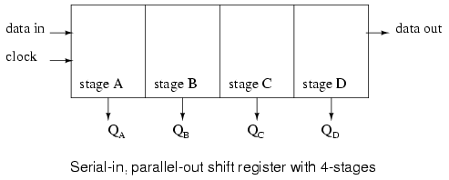
Above, four data bits will be shifted in from "data in" by four clock pulses and be available at QA through QD for driving external circuitry such as LEDs, lamps, relay drivers, and horns.
After the first clock, the data at "data in" appears at QA. After the second clock, The old QA data appears at QB; QA receives next data from "data in". After the third clock, QB data is at QC. After the fourth clock, QC data is at QD. This stage contains the data first present at "data in". The shift register should now contain four data bits.

A parallel-in/parallel-out shift register combines the function of the parallel-in, serial-out shift register with the function of the serial-in, parallel-out shift register to yield the universal shift register. The "do anything" shifter comes at a price– the increased number of I/O (Input/Output) pins may reduce the number of stages which can be packaged.
Data presented at DA through DD is parallel loaded into the registers. This data at QA through QD may be shifted by the number of pulses presented at the clock input. The shifted data is available at QA through QD. The "mode" input, which may be more than one input, controls parallel loading of data from DA through DD, shifting of data, and the direction of shifting. There are shift registers which will shift data either left or right.
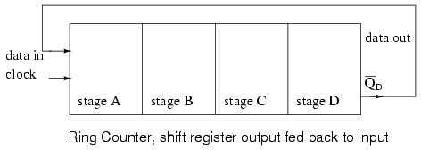
If the serial output of a shift register is connected to the serial
input, data can be perpetually shifted around the ring as long as clock
pulses are present. If the output is inverted before being fed back as
shown above, we do not have to worry about loading the initial data into
the "ring counter".
출처: http://www.allaboutcircuits.com/vol_4/chpt_12/1.html
Translatd by Johnny Koo
'Study' 카테고리의 다른 글
| SPI 통신 (0) | 2013.04.15 |
|---|---|
| my Baby (0) | 2013.04.12 |
| GCC 컴파일 과정 (0) | 2013.03.20 |
| 라플라스 변환 (Laplace Transformation) (0) | 2012.07.11 |
| 2012년 현재 하고 있는 일 설명 (0) | 2012.07.03 |
